Does anyone have any good resources on where to look for PCB design tutorials or troubleshooting services (paid or otherwise)? I’ve designed what I think is a really simple shield to connect the boron to a 2-wire RS485 RTU, but it’s not quite working, and I’m not sure why.
You could start by posting the schematic & board layout here, along with the problems you are experiencing. Be a good way to get lots of eyes on the problem.
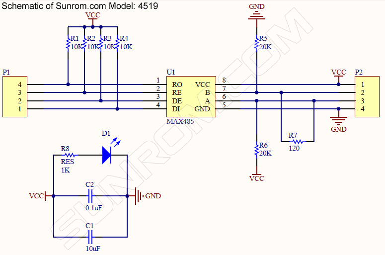
Happy to! Images pasted below. The issue seems to be that the TX signal isn’t reaching the screw terminals, which leads me to believe I’ve connected the RS485 tranciever incorrectly somehow. I’m also! attaching images of the schematics that I worked off of to get this far.
There are a lot of problems.
Did you actually get this produced?
Or are you working from a breadboard?
I used a coupon code to get it produced, because it wound up being not a super different cost from parts alone I wanted, so I figured I’d gamble. They sent me some of the spare parts along with it, so I have those on a breadboard now (though I haven’t yet figured out how to solder legs on to the SMT resistors).
Ok no problem.
For a smaller design like this, it’s probably best to prototype it on a breadboard so you don’t waste the coupon to get a PCB made. It will also help you flush out “bugs” before you draw the schematics and layout the board.
Also, if you are new to designing schematics and layouts it’s always a good idea to get someone to review your work before you get it produced. That’s what these forums are for  (To help each other out)
You might want to get yourself some through-hole parts for your breadboard. You’re asking for more problems if you want to solder legs on SMT parts.
What CAD program did you do your Schematic/Layout in? EAGLE?
Three things leap out to me:
- Looks like you have the wrong pin for gnd on the boron - should be pin 4, not 3.
- I am assuming that the red pour is +5V/USB ?
- You have an unrouted airwire on the layout you posted (the thin yellow line) - that is a connection it knows it needs to make, but there is no trace yet.
Also - you should avoid using differing names for different parts of nets (e.g. USB & +5V, D7 & RTS) - it just makes it hard/error-prone to follow along.
I used EAGLE. I tried to upload it with the images, but it’s not an accepted file type.
and the top row of pins is mirror imaged!
re:the airwire that had been my first concern, but it actually seems to be connected (according to the multimeter anyway).
The red pour is 5v+
You also left out the termination and pull up/down resistors on the RS-485 side - probably not fatal, but undesirable unless you know exactly what you are doing.
If the top connector is flipped (either rotated or mirrored), then the USB/+5V pin will also be wrong, so neither power or gnd are actually connected.
If you fill the polygons in eagle, that will make any airwires go away that are satisfied by the pour.
Can you tell me more about the pull up/down resistor?
How can the nets +5V and USB be connected together if the net names are different? This should throw a DRC error. (I’m unfamiliar with EAGLE so that may be an option?) Anyway if they are conneted:
- Do you have +5V on pin 8 of the 485 chip?
- There is a red trace going from pin 15 to a resistor, then a blue trace going up to the IC through a VIA. Does the blue trace also go to PIN 15? It’s hard to tell from the image.
USB in this case is just a text name (for myself) it is the +5V net.
Pin 8 is connected to +5V
PIN 15 of the Boron is connected to Pin 4 of the IC (TX to TX) via the ground end of the resistor.
Oh, that clears things up a bit thanks. 
I see the only remaining serious issue as GND trying to use pin 3 instead of pin 4 of the boron.
If you break out the rework tools and re-route the ground connection to pin 4, do things get better ?
Isn’t the Boron IO 3V3 only as well?
Good point - you did say there were multiple problems…
You could drop in a SN65HVD75 instead (works @ 3.3V, same footprint), and pull the positive rail from pin 2 (3.3V) instead of VUSB


