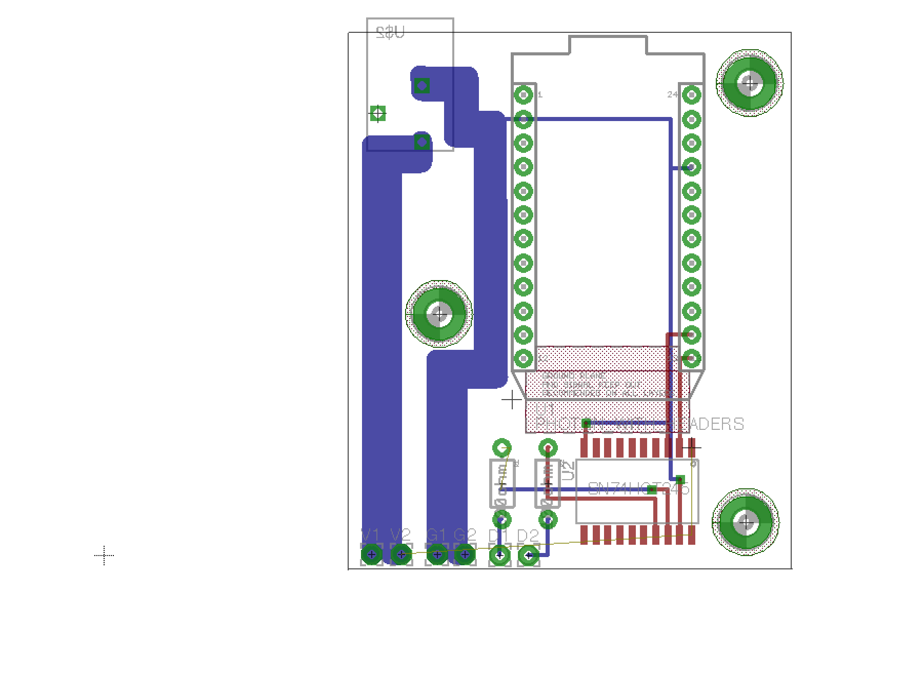
UPDATE Here a look at the PCB I’m building
and here is the sch file:

Any advice would be awesome.
I’d actually keep all copper out the keep-out-area around the chip antenna.
Will you be needing the USB connector in normal use? If not, flipping the Photon around 180° to have the antenna completely free might be an idea.
Adding some decoupling caps wouldn’t harm either.
BTW, aren’t you missing the Vin connection to power the Photon?
Thanks for the advice. I can't believe I forgot the Vin connection and I didn't understand well that area on the Photon I thought I was good as long as I didn't place any components there. I will flip the photon board Also would like to know what type of cap would you recommend.
While you’re at it, why not add some more headers or proto-area so you can hook up other components easily :)?
I’d add a 47µF or 100µF electrolytic and a a 10-100nF ceramic, but I usually sprinkle them however I feel, but @bko or @peekay123 may have more fundamental info which would be best 
If you make all components SMD, you might be able to put the power plug underneat the photon.
Also, where are the neopixels connections :o? Would be neat to have some pads you could solder the strip to.
Hi @Jean-Pierre
Here is a nice read on why decoupling is needed and how to go about it:
http://www.analog.com/media/en/training-seminars/tutorials/MT-101.pdf
The normal capacitors are 0.1uF ceramic and 47uF electrolytic but these values can be changed to suit the board and application.
@ScruffR look at my updated pcb view. I added a 0.1µF on the input of the photon and 2 on the 2 out put. Now I’m not sure on the output to the strip. @bko and @ScruffR mention the 47µF electrolytic should I use that for the strip output.
@Moors7 interesting idea I could add a 3 pad right there on the side of the board and evan add a hole new pin for it. I do have a question my strips are space like this GND, DATA, 5v but I have seen 5v, GND, DATA . Do you know the most common layout?
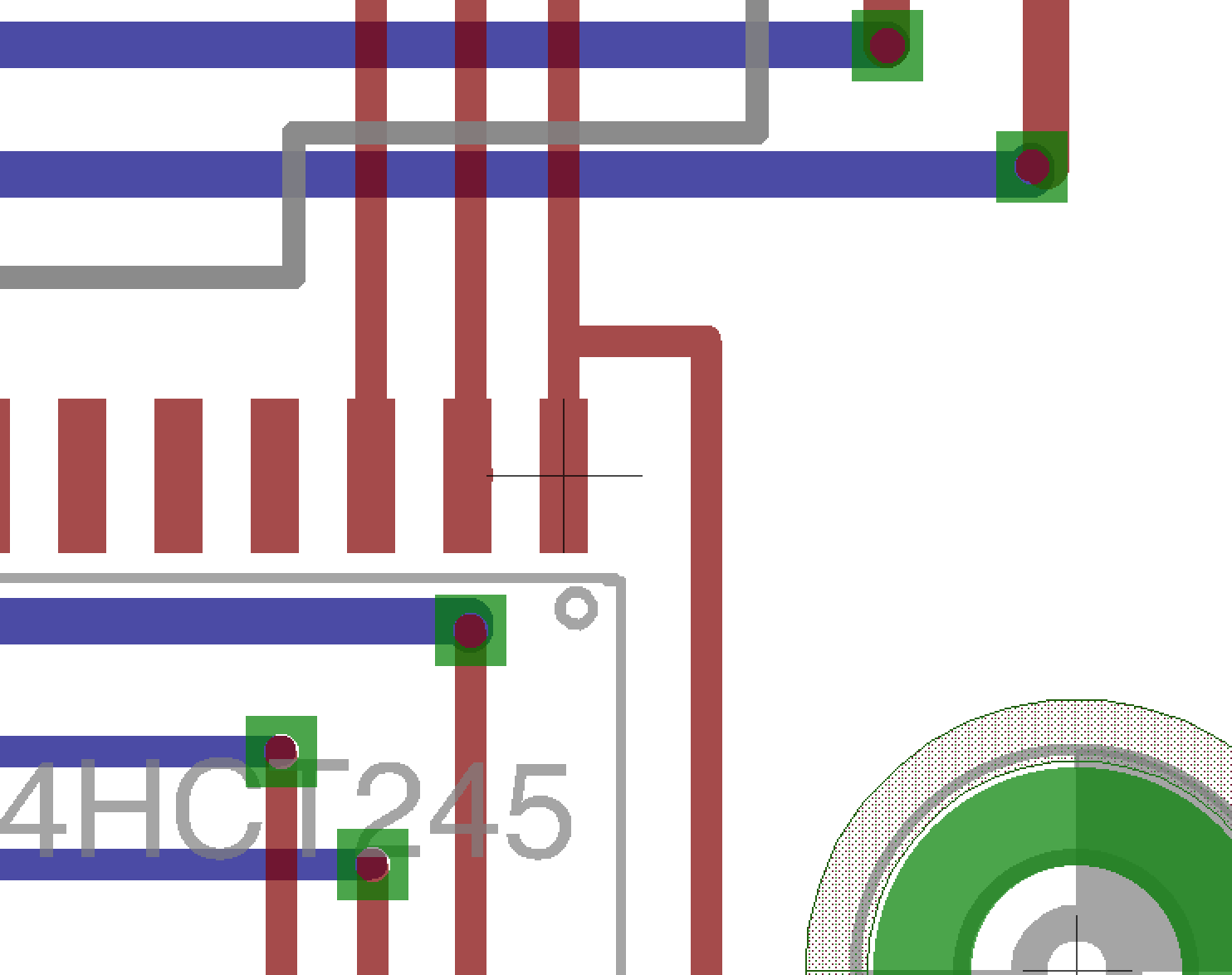
I would fatten up the power traces to the Photon and the other IC as well. It looks like you are using signal width traces (0.012-0.008 inch) instead of nice fat 0.030 or 0.040 inch.
your right I was using .4064mm/.016 inch traces also I just tested the size would that not be a little to big?

You don’t have to make the traces thicker than the pad or land unless you are continuing on to the next IC. In your most recent screen shot, it looks like you could down to the pad/land thickness for the HCT245.
In any case, don’t thicken the pad/land (like you have on the HCT245 above) because you can suck the part off to side when you solder it. Just touch the end of the pad/land with the fat wire.
That’s right–not bigger (but you can go right up to that size if you need it). Just don’t make the pad bigger with the traces that connect to it.
@bko Thank you  I didn’t know that but it makes sense. Could you comment on the decoupling caps? I’m not comply sure about them. And Especially the ones in the middle of the big traces.
You don’t need two 0.1uF side by side like you have on the left side. Can you switch one to an electrolytic?
I don’t see a bypass cap for the HCT245. The one you have on the Photon looks good to me.
ok so you mean add 1 cap for the HCt245 and one 47µF electrolytic to replace the 2 0.1uf cap?
@Jean-Pierre, what is the U$2 connector part number? The traces you have going from that connector to the V1/V2 and G1/G2 pads seems excessively thick for the current you expect to draw. What is the width of those traces?
The u$2 is a power supply connector berral connector type I used a trace carculator for 6amps and thats the width is told me i think it was 1.72mm but im not sure i can’t check right now normal oporation would be 3.5amps but it could go up to 5.5apms
@Jean-Pierre, the barrel connector may only be rated for 3 or 5 amp operation. What is the part number?